
With the development of information technology in China, such as cloud computing, big data, autonomous driving, artificial intelligence, etc., the transmission capacity of optical communication networks has been significantly improved and has become an important component and key carrier base of modern communication infrastructure
Data centers have become an important "computing power base" to promote the digital transformation of society and promote the vigorous development of the digital economy. The country has launched the "East Data West Computing" project, further promoting the development of data centers and increasing the demand for high-performance optical modules and devices. Due to advantages in transmission capacity, integration, cost, and energy consumption, optical chips and modules have become key components of internal interconnection in data centers
The optical modules required for data center applications account for approximately 75% of the market share of communication optical modules. Therefore, data centers have become one of the main application scenarios for optical modules
The development of optical communication technology and information technology is complementary. On the one hand, optical communication devices rely on precise packaging structures to achieve high fidelity output of optical signals, making the precision packaging technology of optical communication devices a key manufacturing technology to ensure the sustained and rapid development of the information industry; On the other hand, the continuous innovation and development of information technology have put forward higher requirements for optical communication devices: faster transmission speed, higher performance indicators, smaller external dimensions, higher degree of optoelectronic integration, and more economical packaging technology.
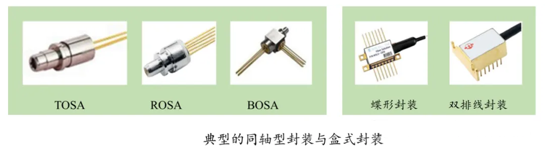
There are various forms of packaging structures for optical communication devices, and typical packaging forms are shown in the following figure. Due to the very small structural dimensions of optical communication devices (typical core diameter of single-mode fibers is less than 10 μ m), any slight deviation in any direction during the coupling and packaging process will cause significant coupling losses. Therefore, optical communication devices need to have high positioning accuracy when aligning with coupled motion units.
The silicon photon optical transceiver is currently the most mature silicon photon device, which includes dedicated silicon chip processors for transmission and reception, silicon photon integrated chips that integrate semiconductor lasers, splitters, and signal modulators, optical sensors, and fiber couplers. It is packaged in a plug and play fiber optic connector and can convert electrical signals from data center servers into optical signals for transmission through optical fibers.

Optical transceiver is currently the main product of silicon photonics, and related technologies continue to improve. The data transmission rate of mainstream products has advanced from 100Gbps in 2016 to 800Gbps in 2023.
Co Packaged Optics (CPO) can reduce transmission signal loss, increase packaging density, and enhance thermal management, making it an important alternative to pluggable transceivers. In the short term, plug-in optical transceivers are still relatively mature products and have advantages in the convenience of system deployment. In the long run, CPO modules will provide better benefits in terms of energy consumption, production costs, and data transmission bandwidth limits.
Silicon photonics will gradually shorten the distance between the optical transceiver module/photon engine and the switch chip, starting from the current mainstream Pluggable Transceiver (TRX), to achieve OBO/CPO, in order to reduce the transmission signal loss of copper wire connections, increase packaging density, and improve thermal management capabilities. Note: On Board Optics (OBO); Co Package Optics (CPO).
The 2.5D hetero integrated packaging structure is adopted for the silicon photonic optical transceiver. Taking the optical transmitter as an example, the hetero integrated packaging integrates the silicon chip, laser module, optical coupler, etc. on the silicon interposer to form a single module.
A silicon waveguide structure is fabricated above the silicon intermediate layer using a mature semiconductor process. Silicon dioxide (SiO2), which has a lower refractive index than silicon, is used to confine the optical signal emitted by the laser within the waveguide structure, facilitating subsequent optical signal transmission and modulation.
Optoelectronic devices are an important component of the electronic information industry and are key and core components of optoelectronic technology. As an important branch of information technology, optical communication technology is a hot topic that developed countries are competing to develop. The rapid development of China's information industry and the increasingly perfect industrial system have also ushered in unprecedented market opportunities for optical communication devices.
This article is reprinted from the internet. If there is any infringement, please contact us to delete it. Thank you!


©2022 - Temperature Forcing Systems-Chengdu ZongLen Technologies CO.,LTD All rights reserved Shu ICP Bei No. 19040265-12 ![]() 川公网安备51012402001121
川公网安备51012402001121