
Electrostatic discharge (ESD) should be the main culprit causing electrical over stress (EOS) damage to all electronic components or integrated circuit systems. Because static electricity usually has a very high instantaneous voltage (>several thousand volts), this damage is destructive and permanent, causing the circuit to burn out directly. So preventing electrostatic damage is the top priority for all IC design and manufacturing.
Static electricity is usually artificially generated, and during processes such as production, assembly, testing, storage, and handling, static electricity may accumulate in the human body, instruments, or equipment. Even electronic components themselves may accumulate static electricity. When people unknowingly come into contact with these charged objects, a discharge path will be formed, instantly causing damage to electronic components or systems due to electrostatic discharge (which is why in the past, when repairing computers, it was necessary to wear an electrostatic ring on the work desk to prevent human static electricity from damaging chips).
So, how to prevent electrostatic discharge damage? Design protective circuits inside the circuit, so that our electronic components or systems can protect themselves from static electricity damage when there is static electricity outside (in fact, installing a lightning rod). According to the different modes of static electricity generation and damage to circuits, there are usually four testing methods: Human Body Model (HBM), Machine Model, Charge Device Model (CDM), and Field Induced Model (FIM). However, the industry usually uses the first two modes for testing (HBM, MM).
Human Discharge Mode (HBM)
Of course, the electric charge generated by human friction suddenly hits the charge released by the chip, causing the chip to burn and break down. The industry also has traceable ESD standards for HBM (MIL-STD-883C method 3015.7, equivalent human capacitance of 100pF, equivalent human resistance of 1.5Kohm), or international electronic industry standards (EIA/JESD22-A114-A). If it is MIL-STD-883C method 3015.7, it specifies Class-1 for voltages less than<2kV, Class-2 for voltages between 2kV and 4kV, and Class-3 for voltages between 4kV and 16kV.
Machine discharge mode (MM)
Of course, when the static electricity generated by the movement of a machine (such as a robot) touches the chip, it is released by the pins. The sub standard is EIAJ-IC-121 method 20 (or standard EIA/JESD22-A115-A), with an equivalent machine resistance of 0 (due to metal) and a capacitance of 100pF. Due to the fact that the machine is made of metal and has zero resistance, the discharge time is very short, almost between ms or us. But the more important issue is that due to the zero equivalent resistance, the current is large, so even a 200V MM discharge is more harmful than a 2kV HBM discharge. Moreover, due to the coupling effect between many wires in the machine itself, the current will interfere and change over time.
The ESD testing method is similar to the GOI test in FAB. After specifying the pin, first apply an ESD voltage to it for a period of time, and then come back to test the electrical properties to see if there is any damage. If there is no problem, add another step of ESD voltage for a period of time, and then measure the electrical properties. Repeat this process until breakdown occurs. At this point, the breakdown voltage is the ESD failure threshold voltage. Usually, we apply three voltages (3 Zaps) to the circuit. In order to reduce the testing cycle, the starting voltage is usually 70% of the standard voltage ESD threshold, and each step can be adjusted to 50V or 100V as needed. In addition, due to the large number of pins on each chip, it will be divided into several combinations: I/O-pin testing (Input and Output pins), pin to pin testing, VDD Viss testing (Input to Output pins), and Analog pin testing.
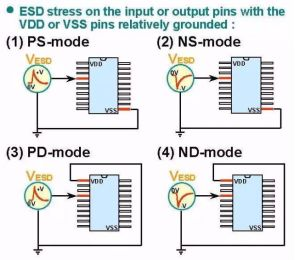
1. I/O pins
It means conducting ESD tests on input pin and output pin separately, and there are positive and negative charges, so there are four combinations: input+positive charge, input+negative charge, output+positive charge, and output+negative charge. When testing input, the output and other pins are all floating, and vice versa.
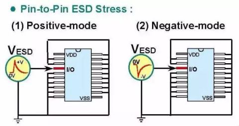
2. Pin to pin testing
Static discharge occurs between pins to form a circuit, but if too many combinations of two pins need to be tested each time, because any I/O that needs to be affected by voltage must first go through VDD/Vds before supplying power to the entire circuit. Therefore, the improved version uses a certain I/O pin to apply positive or negative ESD voltage, and all other I/Os are grounded together, but the input and output are floating at the same time.
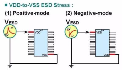
3. Electrostatic discharge between VDD and Voss
Static discharge occurs between pins to form a circuit, but if too many combinations of two pins need to be tested each time, because any I/O that needs to be affected by voltage must first go through VDD/Vds before supplying power to the entire circuit. Therefore, the improved version uses a certain I/O pin to apply positive or negative ESD voltage, and all other I/Os are grounded together, but the input and output are floating at the same time.
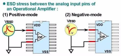
4. Analog pin discharge test
Because many analog circuits have two input terminals for differential pairs or operational amplifiers (OP AMPs), to prevent one from being damaged and causing differential comparison or operation failure, separate ESD testing is required. Of course, only these two pins are tested, and all other pins are floating.
This article is reprinted from the internet. If there is any infringement, please contact us to delete it. Thank you!


©2022 - Temperature Forcing Systems-Chengdu ZongLen Technologies CO.,LTD All rights reserved Shu ICP Bei No. 19040265-12 ![]() 川公网安备51012402001121
川公网安备51012402001121