
With the increase of the scale and complexity of VLSI circuits, the relative number of pins in the chip decreases, which reduces the controllability and observability of the circuit. The circuit test becomes very complex and difficult, and the cost of test generation also increases exponentially. The traditional test methods have been difficult to fully and effectively verify the correctness of the design and manufacturing of complex integrated circuits, resulting in the emergence of the design for testability method.
And testing has become a very important factor in the process of integrated circuit design and manufacturing. It is no longer simply a means of inspection and verification of chip products, but a specialized technology closely related to integrated circuit design, and has become an organic whole with design and manufacturing. Design for testability (DFT) has opened up a practical way for the whole testing field. At present, large and medium-sized IC design companies in the world have basically adopted the design process of DFT, and DFT has become the key link of chip design.
The basic principle of DFT: change the test idea, and change the test method of enumeration and arrangement of input signals (i.e. complete test) into the test of each node in the circuit, i.e. directly test the circuit hardware components, and reduce the complexity of the test. The specific implementation method includes dividing the complex logic circuit into blocks; The use of additional logic and circuits makes test generation easy and can cover all hardware nodes; Add a self-test module to make the test intelligent and automated.
The disadvantage of DFT is that it adds hardware overhead to the design itself, and will also affect the performance of the system to varying degrees, so it must be carefully considered. In addition, the test generation of DFT is usually aimed at the external nodes of gate-level devices, rather than directly at the transistor level.
The difference between "test" and "verification"
When it comes to testing, people often confuse two basic probabilities: "Verification" and "Testing".
Generally speaking, the purpose of verification is to check the errors in the design and ensure that the design conforms to its design specifications and expected functions; Testing is to check the defects and faults produced in the processing and manufacturing of chips.
Verification is to check whether the logic, function and timing of the circuit meet the requirements. Its content is generally functional. As shown in the figure above, verification is to compare the results of Implementation with the definition of Specification. If the verification does not match, the Implementation needs to be changed. Verification is like a barrier in the process of chip design. If the verification fails, all subsequent work cannot be carried out. The verification is generally carried out by simulation technology. The simulation environment is established by computer to add excitation to the circuit under test, analyze the response or explore the information inside the circuit. According to the different stages of verification, simulation can be divided into functional level simulation, gate level simulation and post-layout simulation.
However, a correct design does not guarantee that the chips manufactured will be free from problems, because in the process of manufacturing, chips will always be affected by various uncertain factors, such as environmental interference, inconsistent quality of silicon chips, machine setting deviation, engineer's misoperation, etc. The chips manufactured will not all work normally, so how to detect the chips with manufacturing defects, This is the scope of testing. In the current 7nm manufacturing process of * * *, the line width is very fine, the number of processes is large, and it is very easy to be affected by interference. Manufacturing failures become particularly obvious. Therefore, it is particularly important to increase the strength of testing to ensure that the chip is qualified.
DFT technology is simply to add DFT logic to the chip design, and then after the chip manufacturing is completed, test the chip through the added DFT logic in advance to select the chip with no problems.
DFT technology is more professional, which is a discipline formed to improve the testability of circuits. By adding some hardware circuits, it makes the controllability and observability of nodes in the circuit stronger, and makes the test time shorter and the fault coverage higher.
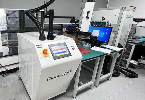
In addition to adding DFT logic to test chips, the TS-580 high and low temperature impact airflow meter developed by Chengdu Zhongliang can perform reliability tests such as characteristic analysis, high and low temperature temperature change test, temperature impact test, failure analysis, etc., such as chips, microelectronic devices, integrated circuits, etc. The performance of the high and low temperature airflow meter has reached a higher standard. The TS-580 takes speed, accuracy and reliability as the basic design criteria and provides a very advanced temperature testing capability. The temperature conversion is from - 55 ℃ to+125 ℃ for about 10 seconds, with a wider temperature range of - 80 ℃ to+225 ℃; Through long-term multi-condition verification, it can meet the requirements of more production and engineering environments. TS-580 is pure mechanical refrigeration, without liquid nitrogen or any other consumable refrigerant.


©2022 - Temperature Forcing Systems-Chengdu ZongLen Technologies CO.,LTD All rights reserved Shu ICP Bei No. 19040265-12 ![]() 川公网安备51012402001121
川公网安备51012402001121