Do you know? The chip in your hand has been punctured, electrocuted, or possibly baked or frozen at high or low temperatures; Each chip delivered to you has undergone rigorous testing and screening, especially for car specification chips, with stricter overall testing coverage and card control indicators.
The process of chip design and wafer factory production involves chemical reactions and physical operations (wafer process). The maturity and performance of different wafer factories may lead to differences in chip functionality and performance, which may not necessarily meet customer needs (such as power consumption and electrical characteristics). Therefore, it is necessary to design a testing plan to eliminate those that do not meet the requirements.
Chip testing generally involves two major steps, one called CP (Chip Probing) and the other called FT (Final Test). CP is testing for wafers, FT is testing for packaged chips, and the process is as follows:
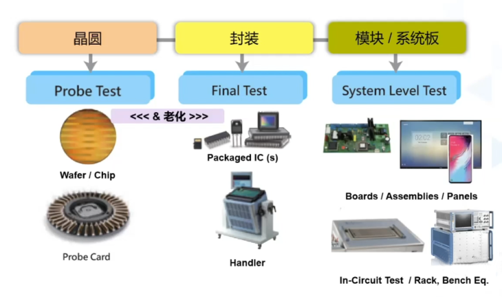
FT is a test for packaged chips, so the leads, substrate, and packaging materials of the chip have been completed. If the wafer DIE is damaged, it will be wasted.
The purpose of CP testing is to screen out bad chip DIEs before packaging.
The following are the yield rates corresponding to different regions of the wafer, and it can be seen that the closer the position next to the wafer, the lower the yield.
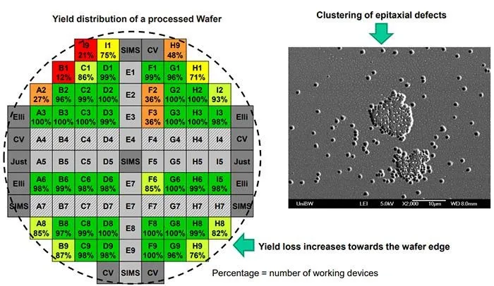
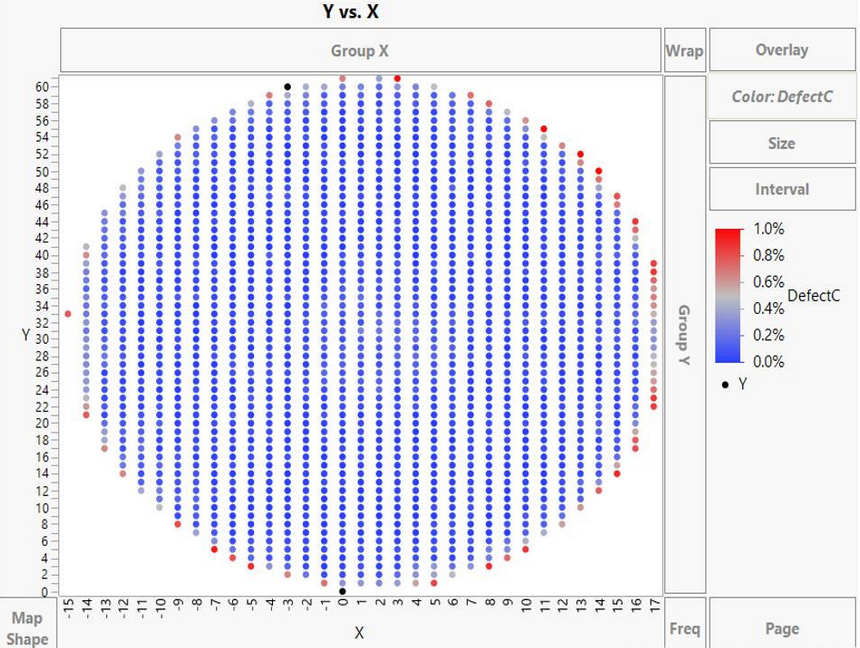
At different stages, CP and FT have different testing objects, limitations caused by differences in testing tools, and different testing focuses. The CP testing phase will cover as many use cases as possible that have a significant impact on yield, such as short circuits, logical functions, and internal storage; Due to the use of probes, CP is generally not suitable for testing high-speed signals, small signals, and high currents, and will be placed in FT for testing;
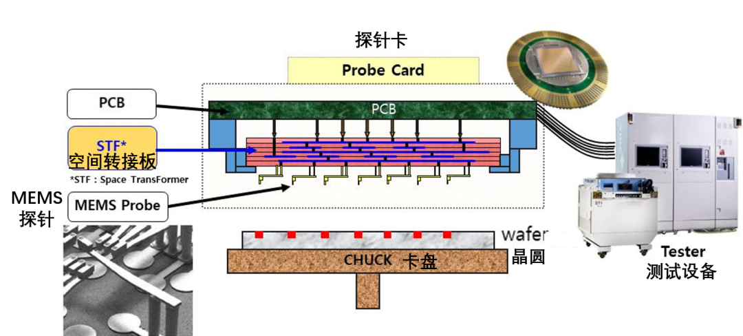
The following is a schematic diagram of CP testing, including the probe card used for testing, the specific operation pictures seen from the microscope on the ATE testing equipment, and the ATE equipment being operated. The ATE device tests each chip on the wafer based on a written program (test case), where the probe's movement distance is average at the 0. Xum level.
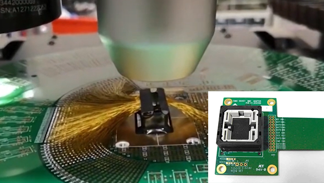
The FT part may be easier for everyone to understand, as it is similar to making test boards in daily life. The main difference may be that FT testing uses Socket sockets (which need to be removed after testing is completed). In order to improve efficiency, a test board can have many such Socket sockets.
This article is reprinted from IC Testing Home. If there is any infringement, please contact to delete it. Thank you!


