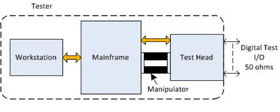
1. ATE=Automatic Test Equipment It is the abbreviation of Test automation, which means integrated circuit (IC) automatic testing machine in the Semiconductor industry. It is used to test the integrity of integrated circuit functions, and is the final process of integrated circuit production and manufacturing to ensure the quality of integrated circuit production and manufacturing.
2. DUT=Device Under Test The equipment to be tested in the semiconductor industry is generally electronic components/chips.
3. PIB=Probe Interface Board Probe interface board: located between the testing machine probe table and the semiconductor wafer or chip. It is a kind of carrier plate, which is mainly used for measuring before semiconductor device packaging and establishing electrical connection with Automatic test equipment (ATE).
4. DIB=Device Interface Board: Between the testing machine and the device
5. PDP=Probe docking plate
6. Handler=IC pick up and place handler. Automatic sorting machine, used for automatically classifying tested chips during testing. After docking with the testing machine and connecting to the interface board, testing can only be carried out. The action process involves the sorting machine's arm placing the DUT into the socket, and the contact chuck is pressed down to ensure that the DUT's feet are in correct contact with the socket. After passing through the interface tester, the tester sends back the binning and EOT signals, and the handler performs the sorting action. The size and number of feet of the customer's product are different, and the handler provides different molds.
7. Manipulator: The semiconductor testing industry's manipulator generally refers to the Test Head Manipulator, also known as the Test Head Manipulator/Test Head Bracket, which facilitates the docking/undocking or adjustment of the test head with the Probe.

8. Probe=Probe station, usually referring to a wafer probe station, which is a machine used for wafer testing during intermediate testing.
In electrical testing, test signals from measuring instruments or testing machines are transmitted to various devices on the chip through probes or probe cards, and then the signals are returned from the devices. The wafer probe station is used to process wafers and make them contact at designated positions on the device. In semiconductor development, wafer detectors are mainly used to evaluate the characteristics, reliability evaluation, and defect analysis of prototype ICs.
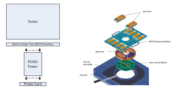
9. Pogo Tower, also known as Probe Tower, is a Chinese probe tower. The probe tower is a mechanically arranged spring contact with controllable impedance connections at the top and bottom, and in the middle. Due to the well-known mechanical and electronic characteristics of the tower, the testing system can compensate for insertion losses and signals.

10.Docking generally refers to the docking method of the board connected to the Probe interface in ATE testing equipment.
Direct docking is an interface docking scheme that does not require a probe tower. Compared with traditional system docking schemes, the characteristics of direct docking are as follows:
Direct Docking System
The interface component is only connected to the test head
The connection between the test head and the probe station is located externally
Conventional System
The interface component is located inside the probe head plate
Connect the test head to the probe table at the interface

11. PCB=Printed Circuit Board, also known as Printed Circuit Board, is an important electronic component that supports electronic components and serves as the carrier for electrical connections of electronic components. Due to its use of electronic printing technology, it is called a "printed" circuit board.
12. PC=Probe Card: The probe card is the interface between the tested chip and the testing machine in wafer testing. It is mainly used to preliminarily measure the electrical performance of the chip before slicing and packaging, and screen out defective chips before proceeding with subsequent packaging engineering. The principle of using a probe card is to directly contact the probe on the probe card with the solder pad or bump on the chip, export the chip signal, and then cooperate with peripheral testing instruments and software control to achieve automated measurement of the wafer. It is very important for the development of early testing and the verification of yield in later mass production testing, and is an important process in wafer manufacturing that has a significant impact on manufacturing costs.
13. Wafer=Wafer. Also known as a substrate, it is composed of pure silicon (Si) and is generally divided into 6-inch, 8-inch, and 12-inch specifications. Wafers are produced based on this wafer. Wafer refers to the silicon wafer used in the production of silicon semiconductor integrated circuits, which is called a wafer due to its circular shape; On silicon wafers, various circuit component structures can be processed and made into integrated circuit products with specific electrical functions.
14. Die Silicon die or bare die refers to a fully functional chip that has not been packaged yet. A wafer is composed of many grains that are separated during the cutting process.
15. Chip - Integrated Circuit (IC) is essentially an electronic circuit that integrates many different devices onto a single silicon chip. It is often referred to as a microchip or a simple chip. Generally speaking, the term chip refers to a small, thin piece of material, sometimes broken off from a larger piece of material. When a chip is not yet packaged, we call it a bare chip. So, most integrated circuits are produced in the form of bare chips on very thin (less than 1 millimeter thick) silicon wafers.
This article is reprinted from an electronic enthusiast. If there is any infringement, please contact to delete it. Thank you!


