
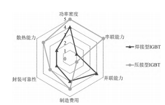
Power module is an important component to realize green energy conversion. Insulated Gate Bipolar Transistor (IGBT), as the power conversion chip with the highest frequency of use, is the device with the highest frequency of failure. Its failure mechanism and detection method have been extensively studied. Reliable packaging provides stable electrical connection, good insulation performance and sufficient anti-interference ability for chip operation, which is an important part of the reliability of IGBT power module. Now, the main packaging forms are soldered and crimped packaging. The two packaging structures are different in power density, series-parallel capability, manufacturing cost, packaging reliability and heat dissipation capacity. Due to the double-sided cooling and failure self-short circuit effect of crimp packaging, it is superior to the soldered packaging in terms of heat dissipation, reliability and series capacity, so it is widely used in high power density occasions, such as high voltage power grids and high power mechanical equipment, but the packaging is complex and bulky. Welded packaging structure is widely used in low and medium power density applications, such as consumer electronics and automotive electronics, because of its simple manufacturing process, low cost and strong parallel capability. The two packaging structures lead to different failure mechanisms, but their essence is that the heat generated by IGBT chip operation is not immediately dissipated, resulting in temperature gradient, and finally the packaging material fatigue leading to failure.
1、 Packaging structure of welded IGBT power module
Since 1975, welded IGBT power module packaging has been proposed and widely used. Among them, Direct Bonded Copper (DBC) is composed of upper copper layer, ceramic plate and lower copper layer. On the one hand, it realizes the fixation and electrical connection of IGBT chip and freewheeling diode, and on the other hand, it forms the main channel for module heat dissipation. The connection between DBC and chip and copper substrate is completed by solder, and the connection between chips and external terminals is completed by ultrasonic bonding leads. In addition, in order to reduce the impact of external moisture, dust and pollution on the module, the entire module is sealed by organic silicon gel.
There are switching losses and conduction losses in the working process of IGBT power module. These losses are dissipated in the form of heat, resulting in temperature gradient in the packaging structure of IGBT power module. Moreover, the coefficient of thermal expansion (CTE) of different materials in the structural layer is quite different, so the cyclic thermal stress is generated, which makes the material fatigue and ultimately leads to the failure of the IGBT power module package. The main failure modes of welding IGBT power module are the failure of bonding line and the failure of welding layer. In practical applications, due to the small power that a single chip can bear, multiple chips are usually combined to form a functional module, or the driver is integrated to form an "intelligent power module".
2、 Failure mechanism of welded IGBT power module package
(1) Failure of bonding wire
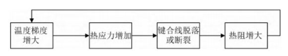
Generally, Al or Cu bonding wires are used to ultrasonically bond the terminal and chip electrode to realize the electrical connection with the outside. Both materials are different from the insulating materials on Si and Si, such as the CTE of SiO2. When the module is working, the power consumption of IGBT chip and the joule heat of the bonding line will increase the temperature of the bonding line, and generate temperature gradient at the contact point and the bonding line, forming shear stress. After a long time in the working state of opening and closing cycles, the stress and fatigue deformation accumulation will lead to cracks at the contact point, increase the contact thermal resistance, increase the joule heat, and increase the temperature gradient, which will eventually lead to the deterioration of the bonding line, form a positive feedback cycle, and finally lead to the bonding line falling off or breaking.
The research shows that these failures are caused by the material CTE mismatch. The fracture of the bonding line occurs at its root, which is the main manifestation of the failure of the bonding line. Some studies have pointed out that the shape of the bonding line can be optimized to improve its reliability. In particular, the higher the height and distance of the bonding line, the lower the stress level of the bonding line and the higher the reliability.
(2) Weld layer failure
The above temperature gradient also exists in the welding layer and adjacent components, which will lead to shear stress. The main forms of weld layer failure are cracks, voids and delamination. In the cycle of opening and closing, inelastic strain will appear in the welding layer as an elastic-plastic material, which will eventually lead to cracks in the welding layer, crack development and delamination of the solder. Cavities are caused by grain boundary voids in solder and reflow soldering process, which is an inevitable phenomenon. With the power cycle, the solder layer is subject to thermal stress, and the voids will also grow. After the failure of the welding layer occurs, the thermal resistance will further increase, resulting in the increase of temperature gradient and the formation of positive feedback, eventually leading to the complete failure of the welding layer.
(3) Electromigration, electrochemical corrosion and metallization reconstruction
There is a layer of Al metal film on the top of the IGBT power module chip to connect with the outside. Under the action of current and temperature gradient, Al metal ions will move along the conductor, such as along the bonding line, resulting in net mass transport, resulting in voids, mounds or whiskers on the film.
With the aging of the device, the air tightness of the silicone gel decreases, and the external substances will contact the Al metal film, causing electrochemical corrosion. The common ones are Al self-passivation reaction, single anode corrosion battery reaction and reaction with contaminated ions.
Metallization reconstruction is due to the difference of CTE value between Al and SiO2 on the chip by two orders of magnitude, resulting in cyclic stress at the interface, which causes diffusion of Al atoms, resulting in mounds, whiskers and voids, and finally plastic deformation, which leads to cracks.
The failure mode of Al film caused by the above three factors will aggravate the fatigue condition at the bonding point, and eventually lead to the falling off of the bonding line or electric field breakdown failure.


©2022 - Temperature Forcing Systems-Chengdu ZongLen Technologies CO.,LTD All rights reserved Shu ICP Bei No. 19040265-12 ![]() 川公网安备51012402001121
川公网安备51012402001121