
1、 Packaging structure
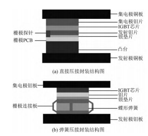
In order to solve the heat dissipation problem of IGBT power module under high power density, Fuji Corporation of Japan proposed u-stack package in 1993. After years of development, two types of crimp package, spring type and direct contact type, have been formed. Direct crimp packaging is to lead out the emitter and collector of the chip through two molybdenum chips, and the gate is led out through a small probe. Therefore, the direct crimping package has double-sided heat dissipation channels, but the structure and materials are more prone to fatigue due to the rigid connection between the components. Spring crimping package is to lead out the emitter and grid through the butterfly spring and grid connection plate. This package reduces the thermal path cross-sectional area of the gate emitter, so the heat dissipation capacity is weaker than that of the direct crimping package. Due to the existence of springs, the pressure balance is better, and the material is not easy to be damaged.
Compared with soldered packaging, crimped packaging has the advantages of low parasitic inductance and short circuit failure. However, due to the mismatch between cyclic thermal stress and multi-layer structure CTE, fretting wear failure, contact surface ablation failure, spring failure and grid oxide layer failure will occur. For multi-chip integrated IGBT power modules, the differences in thermal, mechanical and electromagnetic environment of each IGBT power module will lead to the uneven distribution of heat and current in the module, thus making some positions in the horizontal structure more vulnerable to failure.
2、 Failure mechanism of crimping IGBT power module package
1. Fretting wear failure
The electrical connection of crimping package mainly depends on the pressure between the connecting layers. Therefore, under the action of thermal stress, the horizontal friction phenomenon occurs in each layer, resulting in the increase of contact surface roughness, the increase of resistance and thermal resistance, the increase of temperature gradient, the aggravation of friction, and the formation of a positive feedback cycle. Under this condition for a long time, the contact of crimping package will be separated, resulting in device failure.
2. Contact surface ablation failure
Ablation refers to the phenomenon of ablation damage on the surface of the material caused by the micro-arc of the chip. The reason for this phenomenon in crimping packaging is that there is a bad contact between the interfaces, resulting in the uneven distribution of electric field, and finally causing partial discharge.
3. Spring failure
For spring crimping package, the spring will produce fatigue, stress relaxation and wear with the increase of service time. The common spring failure is the stress relaxation of the grid contact spring, which makes the grid probe contact with the chip poor, resulting in increased resistance and thermal resistance, and finally failure.
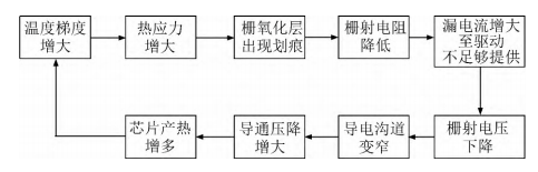
4. Gate oxide failure
No matter what kind of package, there is oxide layer on the gate surface of IGBT chip. Due to the uneven pressure in the packaging process or the effect of thermal stress in the power cycle process, the probe or the molybdenum sheet squeezed the gate oxide layer and caused damage. After the gate oxide layer is damaged, the gate resistance decreases, the leakage current increases, the conduction voltage drop increases, and the chip heat generation further intensifies, and the thermal stress increases, forming a positive cycle.
5. Multi-chip package failure
When there is a short circuit in the crimp package, the Al layer on the chip surface will form an Al-Si alloy with Si under high temperature and high pressure and begin to melt with the previous material. At this time, the IGBT power module conduction is not controlled by the grid. Therefore, in the redundancy design, crimping package is more suitable for series connection. In order to realize the application in high-power occasions, series integrated packaging is often used. At this time, it is necessary to strictly control the thickness difference of each single chip to make its pressure distribution uniform. Due to skin effect and proximity effect, IGBT power modules at edges and corners will bear more current. And the temperature of the chip in the corner of the module is higher than that of the central chip. The existence of this situation will cause the packaging substrate to warp, increase the thermal resistance and aggravate the failure. In the case of series connection, the failure of one chip requires other non-failed chips to bear greater voltage and current, making the whole module more vulnerable to failure.


©2022 - Temperature Forcing Systems-Chengdu ZongLen Technologies CO.,LTD All rights reserved Shu ICP Bei No. 19040265-12 ![]() 川公网安备51012402001121
川公网安备51012402001121