Plasma etching may be the most important process in semiconductor manufacturing, or it may be the most complex among all wafer fab operations, second only to photolithography. Almost half of the wafer manufacturing steps rely on plasma, a high-energy ionized gas, to complete their work.
In order to sustainably manufacture chips with nanoscale accuracy and correct structure, wafer fab equipment manufacturers need to break through the boundaries of plasma physics, material engineering, and data science and provide the required equipment solutions. This is most evident in plasma etching, where plasma etching and photolithography work together to create precise and repeatable features on wafers.
The etching process and lithography technology work together. Etching is usually done before depositing a thin film. Usually, CVD films are coated with photoresist and then exposed using optical lithography using patterned masks (masks). Resist development and reveal patterns. In the plasma etching chamber of a single crystal wafer, chemical substances and ions are usually etched to bombard and remove the CVD film with missing photoresist (in a positive tone resist). After etching, the resist is ashed, wet chemical cleaned, and/or wet etched to remove residues.
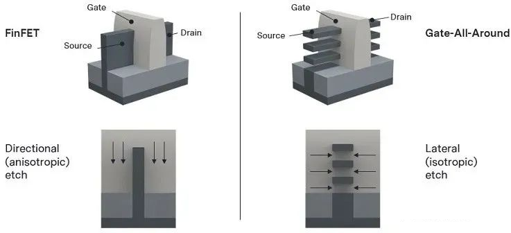
Plasma etching process can be roughly divided into dielectric, silicon, or conductor etching. It is best to use fluoride gas etching for dielectrics such as silicon dioxide and silicon nitride, while silicon and metal layers react best with chlorine. There are basically three dry etching modes - reactive ion etching, plasma etching, and sputtering etching (ion beam). Etching processes are all about the complex interactions between chemical reactants, plasma, and wafer materials. When RF bias is applied to reactive gases, electrons and positively charged ions bombard the wafer to physically remove (etch) the material, while chemicals and free radicals react with the exposed material to form volatile byproducts. Etching can be isotropic (with equal vertical and horizontal reactions), anisotropic (only vertical), or between the two. The transition from finFET to GAA drives the key requirement for isotropic selective etching.

The most concerned indicators for etching engineers are etching rate, contour control, uniformity (entire chip), and etching selectivity, as these all affect yield and productivity. Etching selectivity is simply the removal rate of the material to be etched relative to its underlying layer, such as SiO2 on silicon. It is also advantageous not to remove too much photoresist during etching. But in this case, the pattern is usually transferred to a hard mask (silicon dioxide, silicon nitride, SiOC, TiN) before being transferred to the underlying film. The selectivity specifications range from 2:1 to 1000:1 (highly selective etching). As each new node appears, these specifications become more stringent. As high NA EUVs begin to replace conventional EUVs in the next four years, the focus will be much lower, so thick photoresist cannot be exposed anymore, but it is still necessary to compose the same film thickness below.
For many tool manufacturers, the most challenging step of optimizing the etching process may take a year or more to complete, and process modeling plays a crucial role in the development of etching processes. Can help tool manufacturers shorten their time to market while reducing wafer and mask costs.
This article is reprinted from the internet. If there is any infringement, please contact to delete it. Thank you!


