
MEMS is a manufacturing technology, such as levers, gears, pistons, engines and even steam engines are all made by MEMS. Compared with the chip manufacturing industry, which is more and more familiar to ordinary people, the MEMS technology with the same process as the chip appears somewhat mysterious. What is MEMS?
MEMS is the abbreviation of Micro Electro Mechanical Systems (MEMS). It has a small three-dimensional structure (three-dimensional structure). It is the general name of a system that processes various input and output signals. It is a high value-added component that integrates mechanical parts, electronic circuits, sensors, and actuators on a circuit board by using micro machining technology.
MEMS process is based on conventional semiconductor process flow such as film forming process, photolithography process and etching process.
What are some key technologies of MEMS technology? Next, I'll take you to know more about it.
1. Wafer
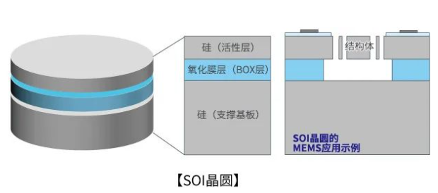
① SOI wafer: SOI is the abbreviation of Silicon On Insulator, which refers to the silicon wafer on which a single silicon layer is formed on the oxide film. It has been widely used in power components and MEMS. In MEMS, oxidation film can be used as a barrier layer for silicon etching, so it can form a complex three-dimensional structure.
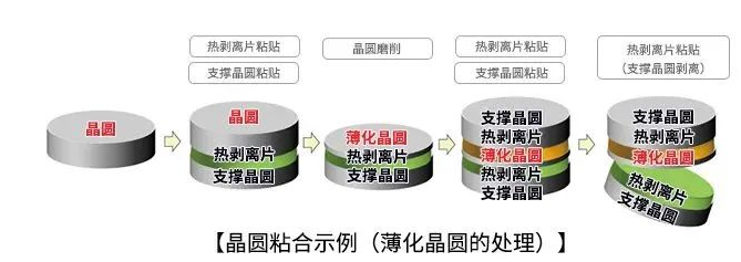
② Wafer bonding/thermal stripping process: thin wafers can be easily processed by using support wafers and thermal stripping wafers.
③ Wafer bonding: Wafer bonding can be roughly divided into two categories: "direct bonding" and "bonding through interlayer".
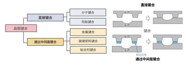
Direct bonding does not use adhesives, etc. It is a bonding that uses the intermolecular force generated by heat treatment to make wafers adhere to each other, and is used to make SOI wafers, etc. Bonding through the interlayer is a bonding method for bonding wafers to each other by means of adhesives, etc.
2. Etching
① Isotropic etching and anisotropic etching: plasma generates ions and other particles by discharging in low vacuum. The technology of etching with these particles is called reactive ion etching. There are charged ions and neutral free radicals mixed in the plasma, which can be used for isotropic etching by free radicals and anisotropic etching by ions.
② Silicon deep etching: Bosch technology, which combines the advantages of anisotropic etching and isotropic etching, has become the mainstream technology of silicon deep etching.
By repeating Si etching ⇒ polymer deposition ⇒ bottom polymer removal, longitudinal deep etching can be performed. The concavity and convexity of its side wall is called "scallop shape" because it looks like scallop.
3. Film-forming
① ALD (Atomic Layer Deposition): ALD is the abbreviation of Atomic Layer Deposition. It is a film forming method that uses the surface reaction with the substrate to deposit atoms layer by layer through repeated material supply (precursor) and exhaust. In this way, as long as there is a gap through which the film forming material can pass, the film can be formed at the side wall of the small hole and the bottom of the deep hole with the nanometer level film thickness control, and the uniform film can be formed during MEMS processing such as polymer deposition during deep etching.


©2022 - Temperature Forcing Systems-Chengdu ZongLen Technologies CO.,LTD All rights reserved Shu ICP Bei No. 19040265-12 ![]() 川公网安备51012402001121
川公网安备51012402001121