
Wafer testing is now an essential part of the wafer manufacturing process. In the early days of semiconductor manufacturing, each chip was tested after it was molded, cut, and packaged. Because of its high cost and low efficiency, a more efficient wafer level testing process was first introduced in 1970, but it was not widely used until the late 1980s. These wafers are subjected to a simple test, using some electronic parameters to determine the proportion of functioning chips, also known as yield, which are then cut into small pieces and packaged individually. However, due to the rapid development of semiconductor applications and related requirements, other parameters are becoming increasingly important, namely temperature and temperature regulation.
Temperature has always been a key parameter in wafer testing and currently has three main applications:
1. According to Arrhenius' equation principle, the semiconductor industry recognizes that temperature can be used to estimate the Life of equipment. Therefore, temperature testing is used to determine the high-temperature Operating Life (HTOL:High-temperature Operating Life).
2. Equipment for specific purposes, such as space, outdoor and automotive applications, need to withstand harsher environments and a wide temperature range. For example, all automotive chips typically need to be tested in the range of -40℃ to +150℃.
3. Electronic testing of high-voltage chips (e.g., high-performance microprocessors) and massively parallel testing (DRAM and NAND chips) are recognized challenges in the industry, requiring rapid and effective cooling to avoid burning out the chips.
As wafer sizes shrink every 1.5 to 2 years as more advanced technology becomes available, these applications are just the tip of the iceberg for wafer testing temperature management needs.
Meeting these temperature challenges in wafer testing often depends on a wafer chuck, which is used to test a variety of temperatures and is therefore often referred to as a temperature chuck. As temperature testing evolves, manufacturers of temperature chucks and probe stands are under increasing pressure to meet industry-required specifications while reducing test time and improving reliability and efficiency.
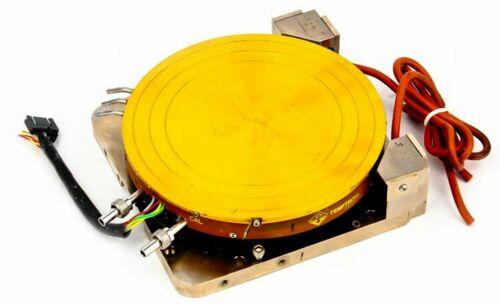
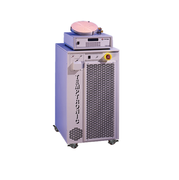
The Temptronic ThermoChuck Wafer testing system uses high and low temperature technology to precisely control the temperature of the wafer chuck and is widely used in wafer level testing for semiconductor processes. Often used with a wafer probe stand, providing a -65 to +300°C high and low temperature test environment, suitable for 150 mm (6 inch), 200 mm (8 inch), 300 mm (12 inch), can be used for Laser Trim Laser Trim and wafer aging burn-in test, such as: Low leakage detection (fA) and high voltage detection (10 kV) are suitable for wafer and chip characteristics description and failure analysis under high and low temperature electrical environment.
Chengdu ChinaCryo Technologies CO.,LTD. can provide technical services such as maintenance, transformation and renovation of refrigeration system / wafer chuck of temptronic thermochuck wafer test system tpo3000 and tpo3500 a.


©2022 - Temperature Forcing Systems-Chengdu ZongLen Technologies CO.,LTD All rights reserved Shu ICP Bei No. 19040265-12 ![]() 川公网安备51012402001121
川公网安备51012402001121